
NEWS DETAIL
Semiconductor quartz, often referred to as semiconductor-grade quartz, is a high-purity form of crystalline silicon dioxide (SiO?) engineered specifically for the exacting demands of semiconductor manufacturing. Unlike standard quartz used in jewelry or countertops, semiconductor quartz undergoes rigorous purification and precision shaping to deliver the thermal stability, chemical resistance, and ultra‐low impurity levels that modern chip fabrication requires.
What is Quartz in the Semiconductor Industry?
In the semiconductor industry, quartz serves as both a structural and functional material. Its crystal lattice of silicon and oxygen atoms grants it exceptional stability at the extreme temperatures and chemical environments inside processing equipment.
Typical forms include:
-
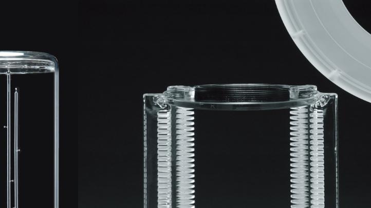
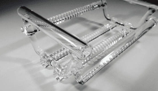
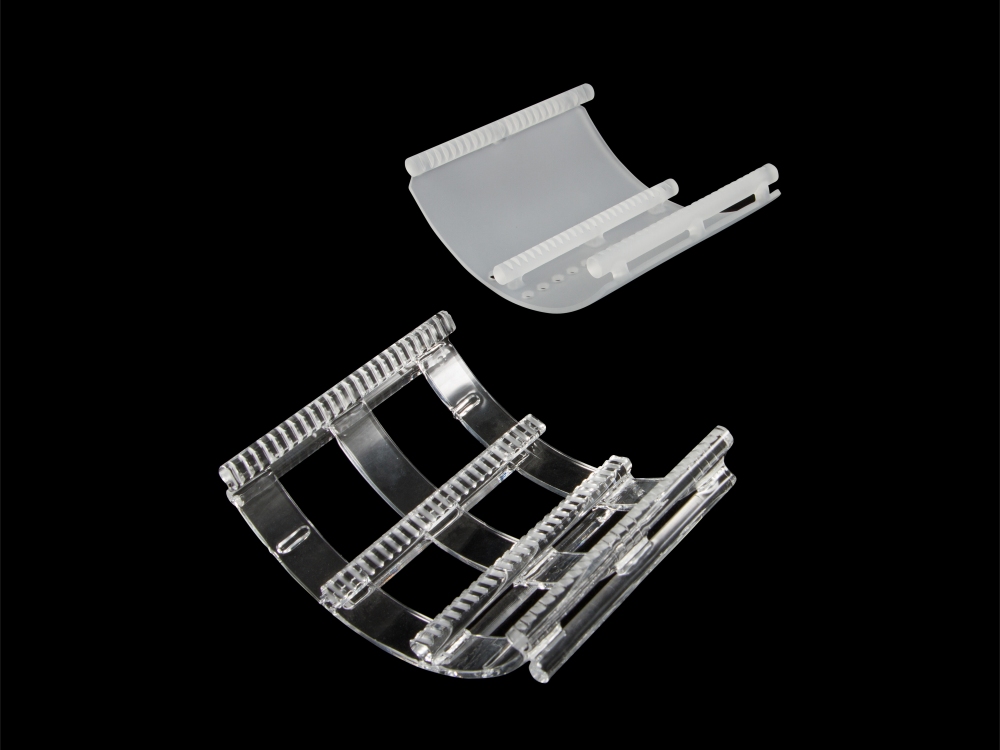
Quartz tubes for diffusion and oxidation furnaces
-
Quartz boats that hold silicon wafers during thermal cycles
-
Quartz plates and rings in etch and chemical‐mechanical polish (CMP) chambers
These components must be fabricated from quartz with purity levels often exceeding 99.9999% SiO?, ensuring that no metallic or ionic contaminants leach into delicate wafer surfaces.
Why is Quartz Important for Semiconductor?
Semiconductor fabrication demands materials that can withstand:
-
High Temperatures
-
Process steps such as diffusion, oxidation, and annealing routinely exceed 1,000?°C. Quartz’s melting point (~1,713?°C) and low thermal expansion minimize warpage or fracture.
-
-
Chemical Aggression
-
Etchants and cleansing agents (e.g., hydrofluoric acid) aggressively attack most materials. Quartz’s chemical inertness prevents container degradation and wafer contamination.
-
-
Ultra‐Low Contamination
-
Even parts‐per‐billion levels of metal ions or hydroxyl groups in quartz can create defects on nanoscale transistors. Semiconductor-grade quartz is manufactured in cleanrooms and undergoes acid leaching and high‐temperature baking to drive out impurities.
-
These attributes translate directly into higher yields and more reliable device performance, making quartz indispensable for front‐end and back‐end process steps.
Applications of Semiconductor Quartz
Semiconductor quartz components appear throughout the fab:
-
Diffusion & Oxidation Furnaces
Quartz tubes house wafers as dopants diffuse or as silicon dioxide grows on wafer surfaces.
-
Chemical Vapor Deposition (CVD) Reactors
Quartz liners and showerheads distribute precursor gases uniformly during thin‐film deposition.
-
Etching & Cleaning Tools
Quartz parts resist plasma or wet‐chemical attacks, preserving tool life and process consistency.
-
Annealing & RTA (Rapid Thermal Anneal)
Quartz plates and supports help achieve uniform temperature ramps and cool‐downs crucial for crystallinity and dopant activation.
-
Quartz Windows & Viewports
High‐transparency quartz enables optical monitoring, laser alignment, and in‐situ spectroscopy without introducing contaminants.
By tailoring geometry, wall thickness, and surface finish, manufacturers optimize heat flow, gas dynamics, and mechanical strength for each application.
How is Semiconductor?grade Quartz Made?
Producing semiconductor?grade quartz involves several critical steps:
-
Raw Material Selection
-
Start with naturally occurring or synthetic high‐purity quartz crystals. Synthetic routes (e.g., hydrothermal growth) can yield extremely low‐impurity boules.
-
-
Crushing & Milling
-
The raw crystals are ground to precise grain sizes under clean conditions, avoiding metallic tooling to prevent contamination.
-
-
Shaping & Sintering
-
Powder is pressed into preforms, sintered at high temperatures to densify, then machined into tubes, boats, or custom geometries with diamond tools.
-
-
Chemical Leaching
-
Acid baths (nitric, hydrofluoric) remove residual metal ions; repeated rinses and deionized‐water soaks ensure parts meet ionic‐contaminant specs (often <1?ppb).
-
-
High?Temperature Annealing
-
A final bake at 1,200–1,400?°C drives off hydroxyl groups and relieves internal stresses, improving thermal shock resistance.
-
-
Cleanroom Packaging
-
Finished components are packaged in Class?100 or better clean environments to maintain purity until installation.
-
Each step is tightly controlled and monitored via spectroscopic and analytical techniques (e.g., ICP?MS, FTIR) to certify the quartz’s suitability for semiconductor use.
Conclusion
Semiconductor quartz stands at the heart of modern chip manufacturing, delivering the purity, durability, and precision necessary for nodes at 5?nm, 3?nm, and beyond. From diffusion tubes to CVD reactors, its unmatched thermal and chemical resilience minimizes wafer defects and maximizes fab yields. As device geometries continue to shrink and process windows tighten, innovations in quartz synthesis and processing will remain pivotal in pushing the boundaries of semiconductor performance.
Whether you’re a fab engineer seeking optimal tool life or a purchasing manager sourcing high‐purity materials, understanding semiconductor quartz is essential to ensuring your manufacturing processes stay ahead of the curve.